Introduction
After studying digital electronics and digital systems design, I set out to implement a real-time parallel hardware solver for the Finite Element Analysis (FEA) of a square drum head on an FPGA, completely from scratch. This device simulates a square drum head being excited by a mallet and produces an audio output in real-time of the drum being struck and decaying. It accomplishes this by computing the solution to the 2D Wave Partial Differential Equation (PDE) in a massively parallel fashion in the FPGA fabric. The algorithm also models non-linear tension effects of deflecting a stretched membrane, which necessitates a numerical method instead of an analytical method. This project also features a software application running on the ARM Cortex A9 embedded hard processor which allows the user to simulate drum strikes with various parameters at different positions on the membrane (using a mouse), and also provides a visualization of the membrane excitation by interfacing directly with the RAM blocks in the FPGA fabric, which makes for a pretty cool interactive demo!
Demo
System Overview
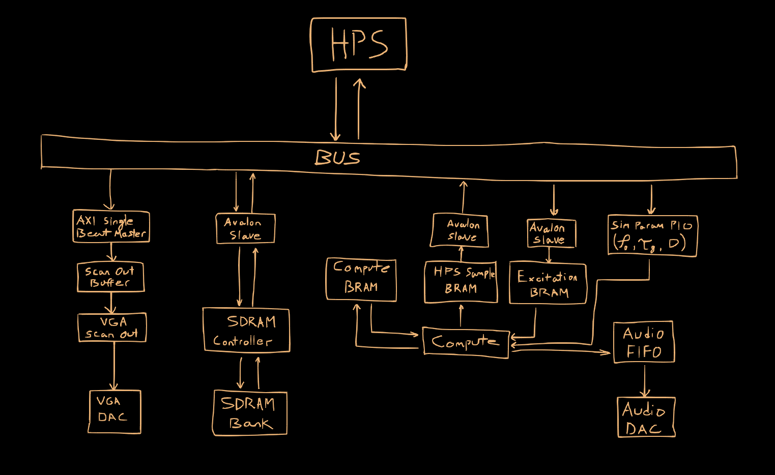
This project was implemented on a Terasic DE1-SoC Cyclone V development kit, which features an embedded Cortex A9 hard processor system (HPS). The hardware design was implemented from scratch in VHDL (excluding the AXI bus interfacing with the HPS), which includes the “compute engine” solving the 2D wave equation, audio FIFO interfacing with the digital-to-analog (DAC) audio converter, custom SDRAM controller (interfacing with offboard SDRAM for storing framebuffers), Avalon Bus Slave for writing framebuffers from the HPS, Avalon Bus Slaves interfacing with FPGA BRAM for triggering membrane excitation from the HPS and reading back simulation results for visualization, Single Beat Pipelined AXI Master for reading framebuffers, and VGA scanout for displaying framebuffers. The software component was implemented in C++ and processes user input (mouse) for interacting with a simple GUI for the simulation parameters (strike velocity, membrane pitch, membrane sustain, and the non-linear tension modeling parameter), exciting the grid with a simulated mallet, reading back the real-time simulation and visualizing it with a (simple) software renderer which writes to SDRAM acting as VRAM through a custom SDRAM controller implemented in the FPGA fabric.
Math Background
In order to reign in the length of this post, I’ll skip over setting up the 2D wave equation problem and solution and jump ahead to converting the solution into an iterative solution. (I’ll make some of my notes available here)
See also this document on finite difference methods for solving the wave equation
We can utilize the Taylor Expansion to convert the differential equation into a difference equation, giving us an iterative solution.
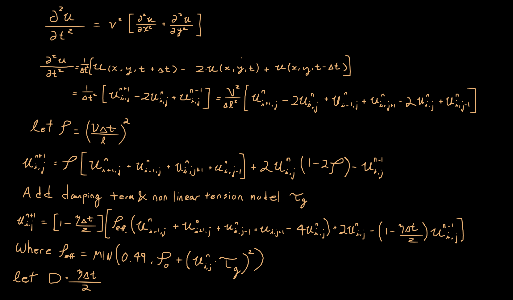
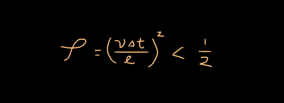
The limitation on ρ being clamped to 0.5 comes from a criteron known as the Courant Condition. This condition is derived from Von Neumann Stability which is a method for testing the stability of an explicit numerical iteration method by testing how the system behaves with various modes (frequencies) of sinusoids being passed through it. If any of the modes demonstrate positive feedback, the system is unstable. The Courant Condition describes a constraint on how fast a wave can propagate on the surface such that it does not alias. This is similar in principle to Nyquist/Shannon sampling theory, but applied to two dimensions. Basically, if the time step is too large, or the velocity of the wave is too high, then you will get aliasing. Thus, you must make sure your time step is small enough, and the propagation speed on the surface small enough that it doesn’t cause aliasing.
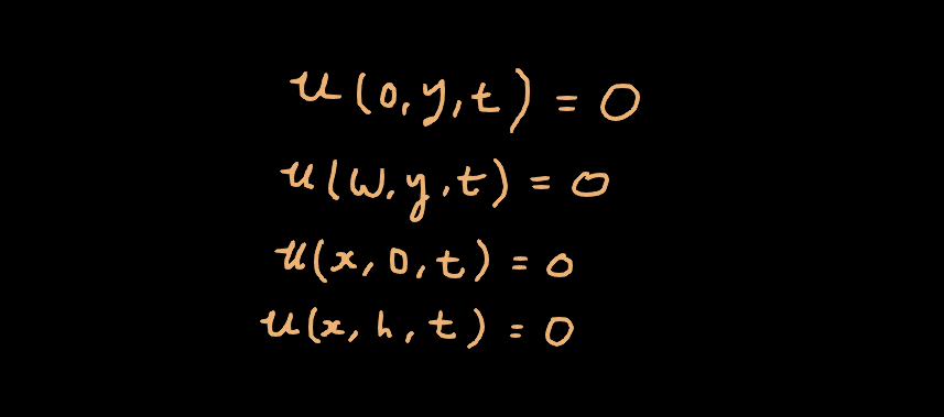
The boundary conditions of this problem are straight forward, they are simply fixed at all four edges.
In order to test this solution, I initially implemented it in matlab. This proved to be much too slow for simulation so I rewrote it in C++, output the audio samples as a csv file and then loaded them into matlab for testing playback and analysis. The naive single-threaded C++ implementation was fast enough for my purposes of fiddling around with the various parameters for medium sized grids. Here’s an example of a 100x100 node simulation:
Hardware Design
The goal of this design is to be able to simulate a large grid of nodes and update the state of the ‘displacement’ of the membrane at each node, and once all nodes have been updated, produce some sort of sampling of the state at that point which can be fed to the audio FIFO. One thing to consider is that as the dimensions of this grid increases, the area of the grid increases quadratically! We need to factor this into the design and make sure it is scalable. The larger we can make the grid the more accurate the simulation will be. At each iteration step, we need to update all nodes in the grid inside the clock period of the audio clock so we have a new sample ready in time for the DAC.
The first step in the hardware design is weighing what kind of requirements we have for computational complexity, and what resources are available in the hardware. Taking a look at the FEA equation, we have a lot of adds/subtracts, a multiply by 2 and 4 (which can be reduced to shifts), and a couple multiplies. The damping factors can be applied via shifts (by strategically picking values of η such that the damping term is a power of 2). But, since we are modelling non-linear tension effects, which are dependent on the current displacement of the membrane (as the membrane becomes more displaced, the tension on it increases). This means we need an actual multiplier to compute this, and can’t just reduce the complexity of the problem by replacing it with shifts. In practice we can just convert the multiply by two to an additional add, and we can eliminate the multiply by four by distributing the subtraction of that term across the other terms. This reduces the number of arithmetic operations to just add, subtract, and multiply. Which is great because then we don’t need to synthesize any logic for shifts.
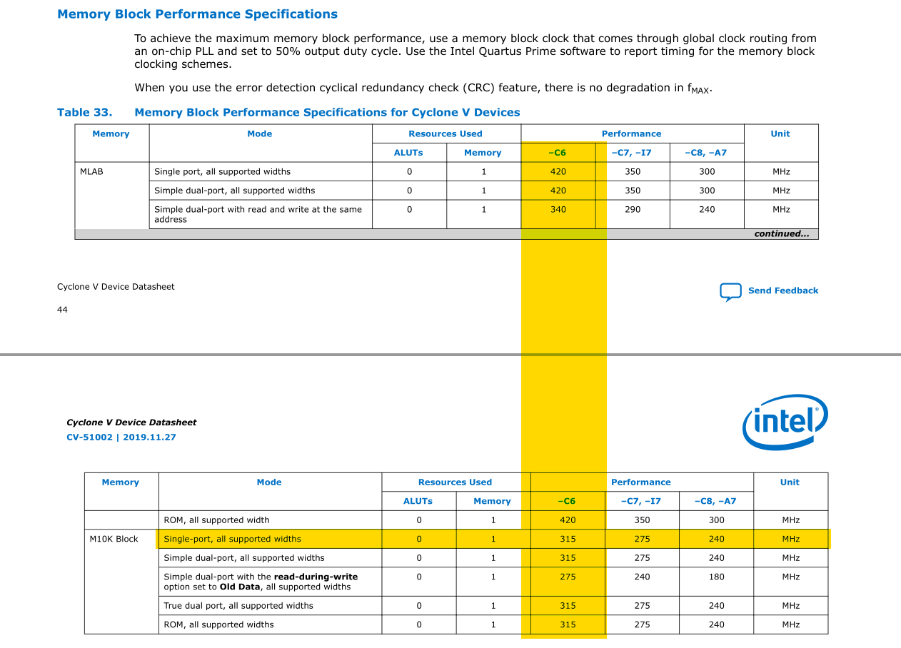
The FPGA has built-in DSP blocks with hard multipliers, and we definitely don’t want to synthesize multipliers out of logic blocks because that will use a lot of logic elements and have a severely negative impact on how fast we can run the system clock. Let’s get an idea for how many hard multipliers we have access to by taking a look at the data sheet.
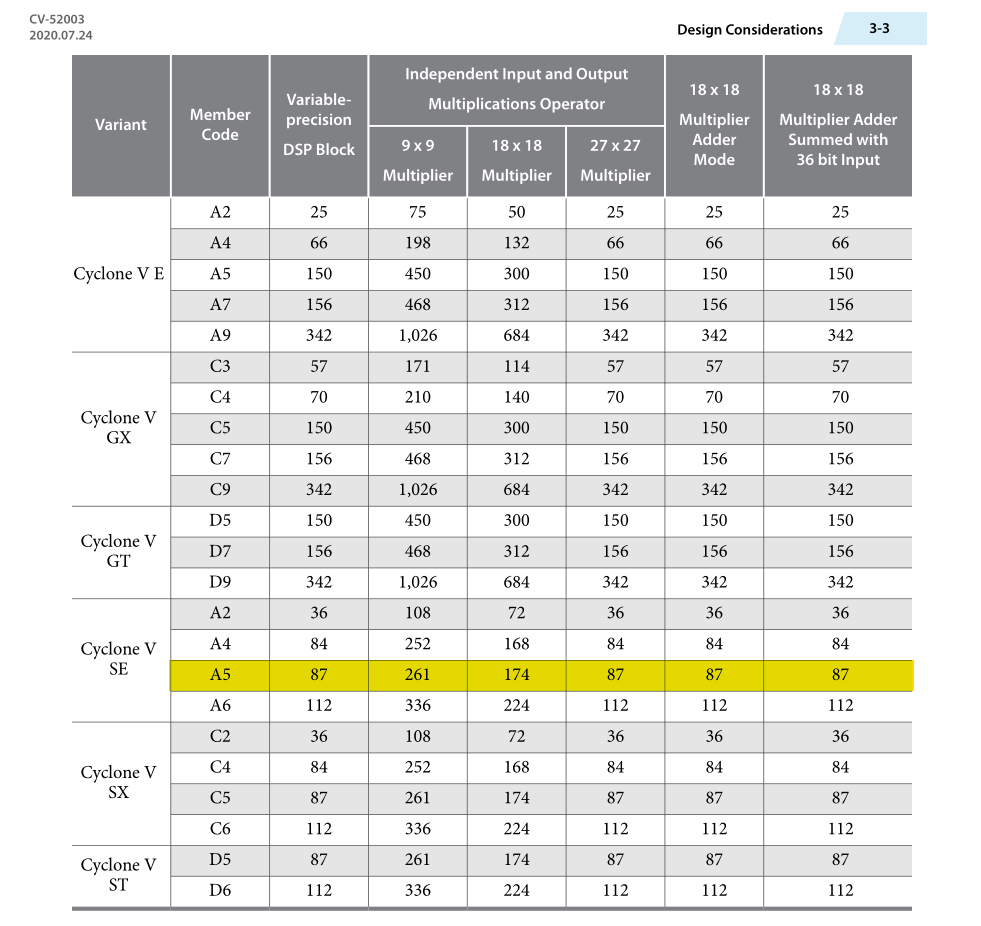
Based on the data sheet for our Cyclone V variant, we have access to 174 multiplier units at 18-bits of precision (2 per DSP block), or 87 multipliers at 27-bits of precision (1 per DSP block). We also need to store the results (compute memory in the system diagram). Since we want this to be as fast as possible to solve the largest grid, using external DRAM with serial memory access would be much too slow. We’ll use the embedded block RAM (BRAM) for this purpose.
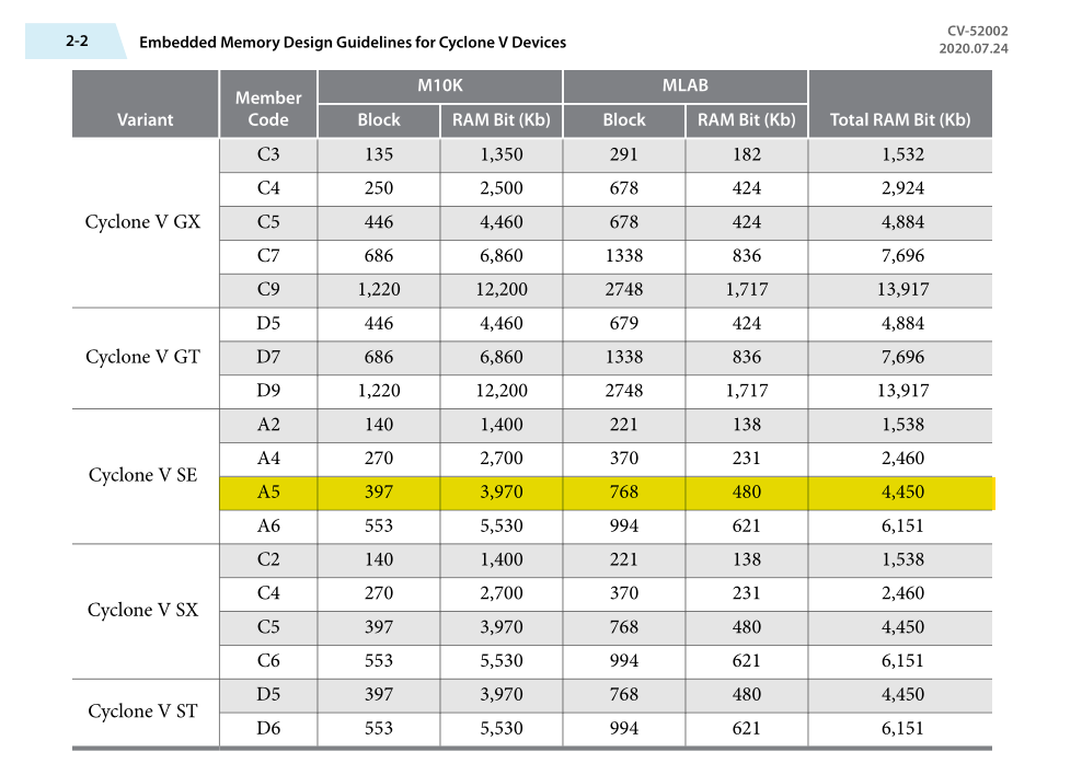
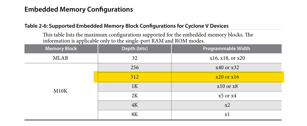
For each node we’re going to store in the grid, we need storage for writing the current computation, and the results of the previous two time steps. i.e., we need three “words” for each node. So each M10K block can store 170 nodes at 18 bits (512 20-bit words), or 85 nodes at 27 bits (256 32-bit words).
Now that we have an idea of the budget for hardware resources, we need to get an idea for our computational budget.
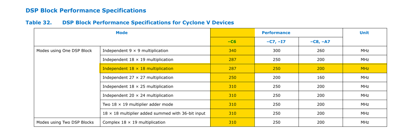
The sampling rate of the audio DAC is 48 KHz, which means we need to produce a new sample every 20,833 ns. Based on the data sheet, the DSP blocks should be the limiting factor for clock speed. If we are able to clock the system clock at the DSP performance limit, we will have 5979 clock cycles at 18 bits or 5208 clock cycles at 27 bits. And remember, this budget is divided across all nodes in the grid. Suppose one node takes 20 cycles to compute, then a serial solution would only be able to solve 298 nodes per cycle at 18 bits (i.e a ~17x17 grid, which is quite small).
Compute Engine
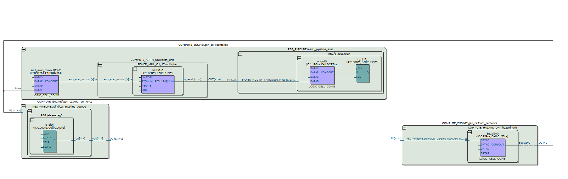
Here is the basic structure of my solution to the problem
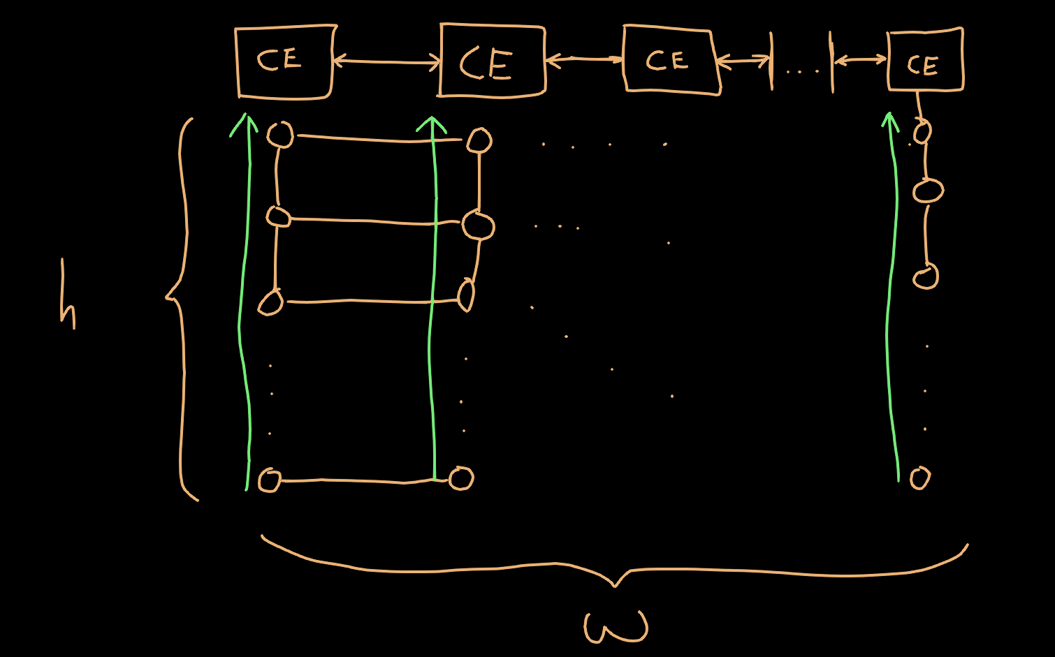
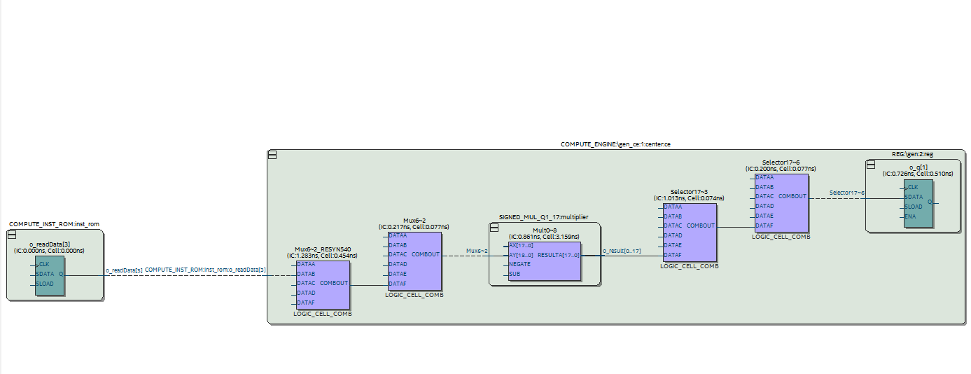
My approach to this problem is basically modelling the computation like you would for doing ‘SIMD’ (single instruction multiple data) “wide” vector operations. The idea here is to instantiate a bunch of what I am calling ‘compute engines’ (although perhaps automata might be more appropriate), and have them operate in lock step with one another. Then, we can allocate one multiplier unit to each compute engine. Each compute engine will be responsible for computing all the results of a column of nodes. Since they are operating in lockstep, they can broadcast their previous [n-1] value out to the adjacent compute engines. If we assign a multiplier and an M10K block to each compute engine, we could simulate a 170x170 square grid of nodes at 18 bits, with each engine being responsible for computing 170 nodes. This results in a budget of 35 cycles per node. If we assume one cycle per arithmetic operation, this gives us a lot of breathing room to downclock the system clock in order to meet timing constraints.
Here is the structure of the compute engine itself
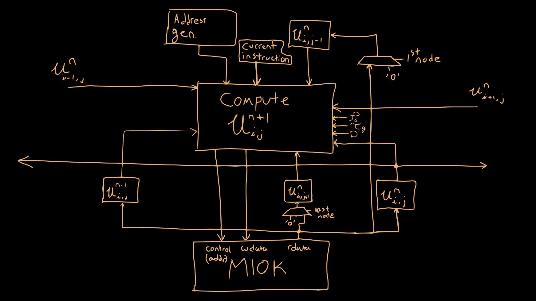
To compute each node, we need to perform the following steps:
- Load the previous time step’s results into all the ‘u’ registers
- Execute the compute sequence to calculate the node at the current time step
- Store the result back to memory
The results of the previous timestep are broadcast out to the adjacent compute engines to the left and right. In order to satisfy boundary conditions, the first and last compute engines will always see adjacent values of “0” for (i-1) and (i+1) terms (respectively). Additionally, all of the engines will need to multiplex in zeros to the (j-1) and (j+1) terms when computing the first and last nodes in the column (respectively). Since all the engines operate in lockstep, we can broadcast a ‘base’ memory address to base the reads/writes on (every engine will read/write to the same addresses within their respective memory block). We will also broadcast an instruction for the engine to execute, as well as the constants to use for computation.
Another thing to note is we also need to ‘juggle’ around the memory locations so that the oldest node grid will be overwritten with the new values, and then reads will come from the previous two grids. This is akin to doing pointer swaps in the software simulation. This is done by generating a ‘base address’ as well as three ‘offset’ values for step [n+1], [n], and [n-1]. Since the grids are not powers of two, I figure it was most efficient to interleave the grids so that the offsets just modulate between 0, 1, and 2. Then after all nodes have been updated we can swap the offsets, so that [n] takes the [n-2] offset, [n-1] takes the [n] offset, and [n-2] takes the [n-1] offset.
Timing Analysis
Timing constraints effectively describe what portions of the design will execute at what clock frequencies. The timing constraints is utilized by the compiler and impacts how it will utilize resources and lay things out in the FPGA. It will try to arrange the configuration to meet the timing constraints specified. Put simply, all elements in hardware add delay to a signal propagating from one element to the next, and the cumulative delay from one memory element (register/flip flop) to the next must be less than the period of the clock driving those memory elements. The timing constraints are also utilized by the ‘timing analyzer’ which is a diagnostic tool for analyzing various timing paths in the design. It will tell us whether the final hardware design achieved by the compiler meets the constraints specified originally. We will need this as we scale the design up to know if the design will meet the target clock frequencies.
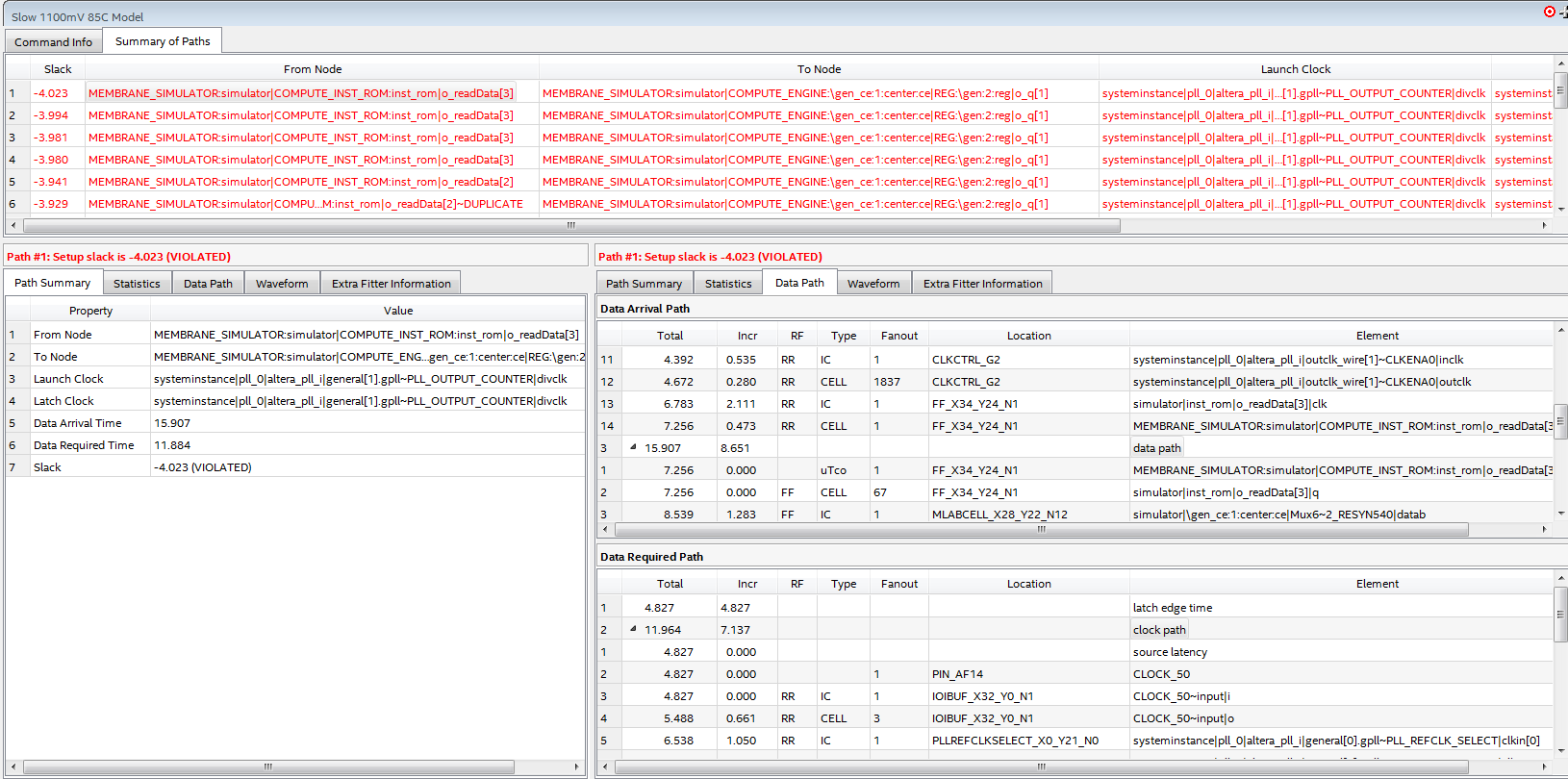
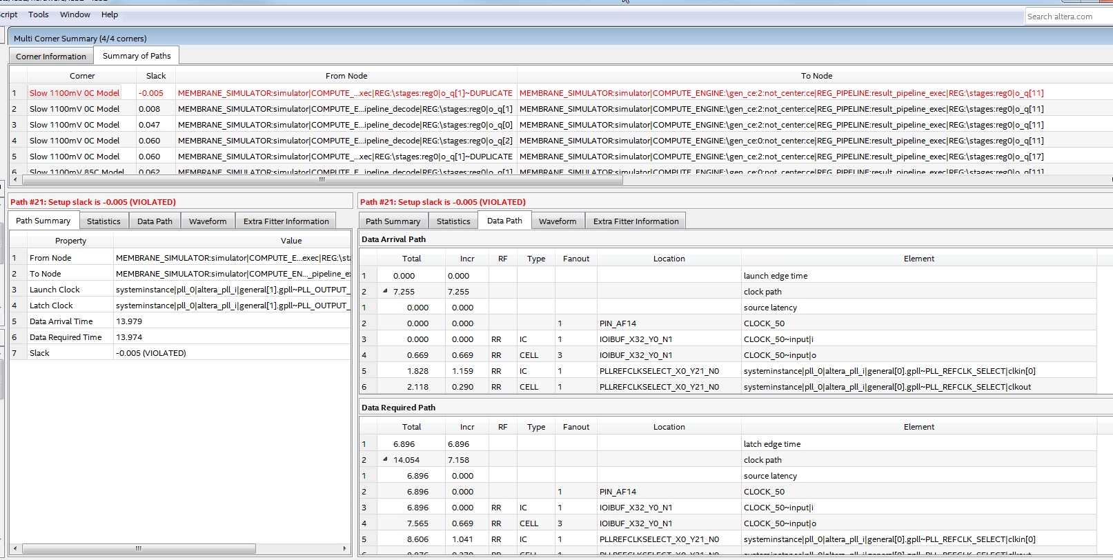
When attempting to scale up the initial design to the target clock rate to support a larger grid size, the design failed to meet timing, by a significant margin, due to a critical path through the multiplier. Even though the propagation delay of the multiplier can support a clock rate of up to 287 MHz, this would only be true if it was directly registered on the input and the output. Delay added by surrounding logic elements caused the timing to fail. The margins were rather substantial, indicating that due to my lack of experience I am severely underestimating the propagation delay of logic elements and interconnects.
Here is the timing analysis, where the critical path through the multiplier is failing (setup) timing by ~4 ns, as well as the critical path.
I decided I would try pipelining the design of the compute engine. This way we can minimize the amount of combinational logic adjacent to the multiplier, resulting in a higher potential clock rate. The cost of this is additional complexity as well as additional overall latency, as we will need to wait for the pipeline to flush the final result before being able to write it back to memory. There’s definitely room for some additional sophistication here by also ‘pipelining’ computations in between nodes, such that we can begin loading values needed to compute the subsequent node while waiting for the result of the current node to exit the pipeline. But, I haven’t taken the time to implement that.
Here is a diagram of the pipelined compute engine architecture
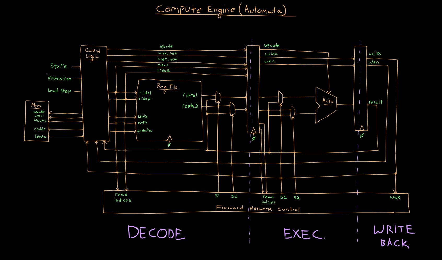
This improved the slack from -4 ns to -2.2 ns, but unfortunately I could still not close timing at a clock rate necessary to support a 170x170 grid. Even after pipelining there was still a substantial amount of delay caused by the forwarding network, which is necessary to forward results to other stages in the pipeline before being written back to the register file.
Here is the offending critical path through the forwarding network and multiplier
I decide to rework the requirements slightly by reducing the number of target nodes to compute such that we could reduce the clock period by 2.2 ns. I reduced the target grid size to 112x112 nodes and 145 MHz clock. At this point point timing was successfully met!
Fixed Point Precision
I ended up choosing 27 bit words using a Q3.24 fixed point format, instead of the initially chosen 18 bit words in a Q1.17 format for a few reasons. After updating my software simulation to perform computations in fixed point instead of floating point I realized I had mistakenly assumed that truncating results would not be an issue. The truncation caused a DC bias in the result due to always rounding results in one direction.
Frequency analysis of an example of a 49x49 grid, at 18 bits (Q1.17), with truncating the result:
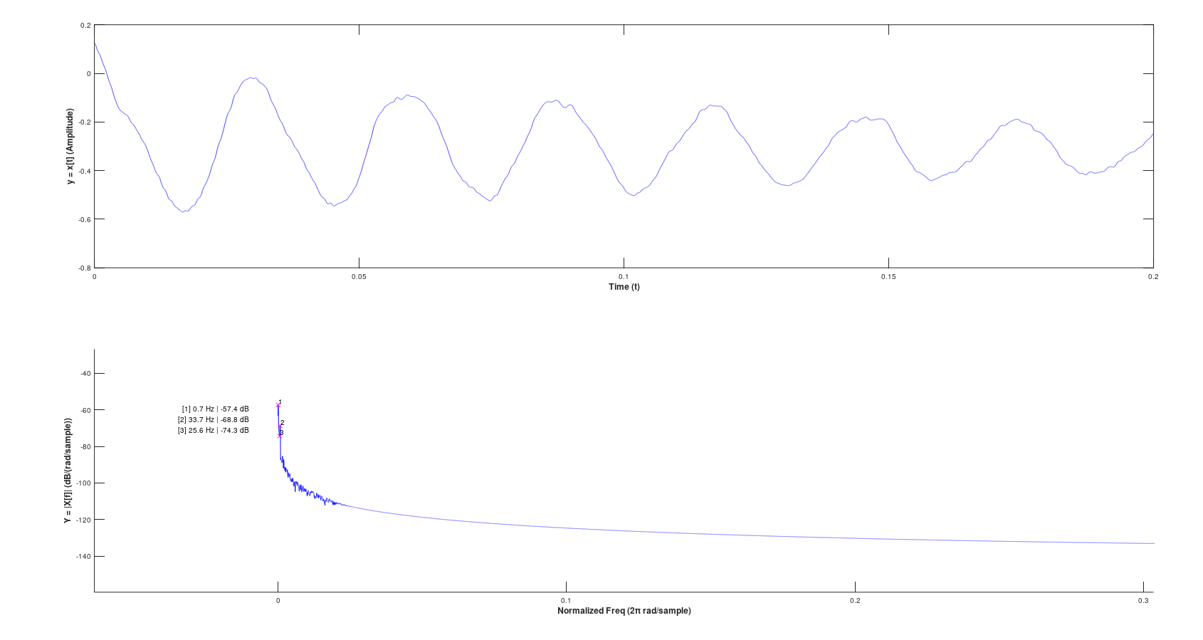
Versus rounding the result
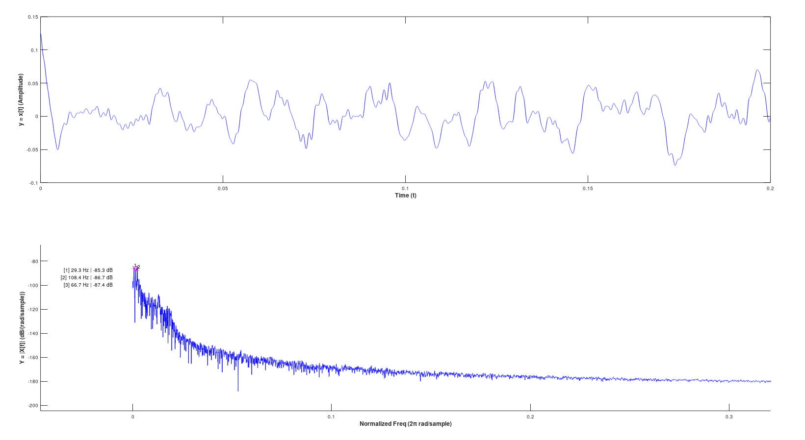
As you can see, the difference in complex frequency content is drastically different, and the DC component is eliminated.
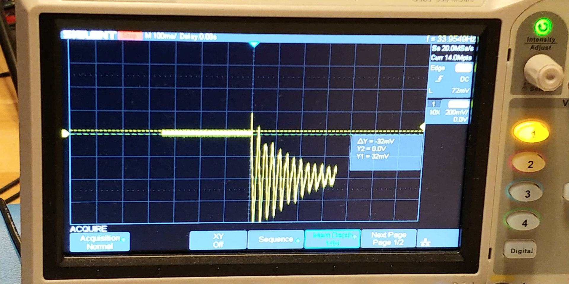
Additionally, here is an example of the output from the physical DAC clearly showing the DC offset on an oscilloscope.
Unfortunately rounding in the DSP block can only be implemented on the output of one of the multipliers of the DSP Block (there are two multipliers per DSP block with 18 bit operands), therefore it makes sense to configure the DSP block as a single 27-bit multiplier. This also allows us to allocate some additional bits above the binary point to mitigate risks of overflow. If any of the arithmetic overflows (e.g., some intermediate value) the results become completely undefined and the simulation becomes completely unstable (which is really bad).
In order to support this I had to reduce the grid size to 85x85 nodes to fit inside a single M10K memory block per compute engine (8192 bits at 32-bits per word, storing 3 grids)
Verification
3x3 Grid
In order to verify the hardware implementation, I compared the results of the software simulation, hardware simulation, and actual audio output from the implementation running on the FPGA. I’ll note the software simulation was done with floating point, not fixed point, so the results do not exactly match, but you can see the fundamental frequencies do indeed match between the software sim and the hardware sim.

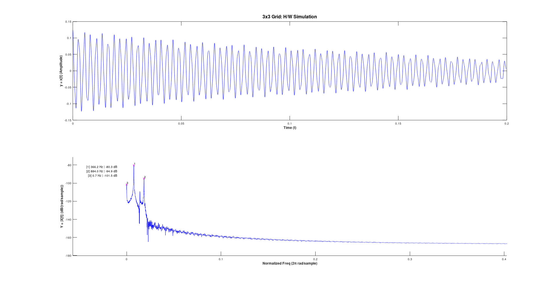
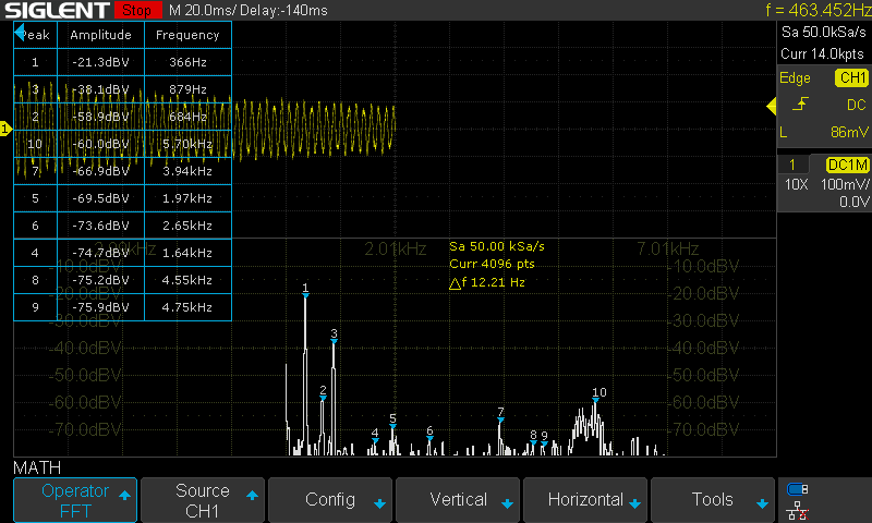
As you can see in the simulations, we’d expect the fundamental frequencies of the tone to be at 366.2 Hz and 883.3 Hz. In the actual hardware output we can see the fundamental frequencies are measured at 366 Hz and 879 Hz.
87x87 Grid
Performing the full hardware simulation of such a large grid would be far too time consuming. Here I just compare the 18 bit fixed point software simulation against the actual hardware synthesis, with rounding enabled.
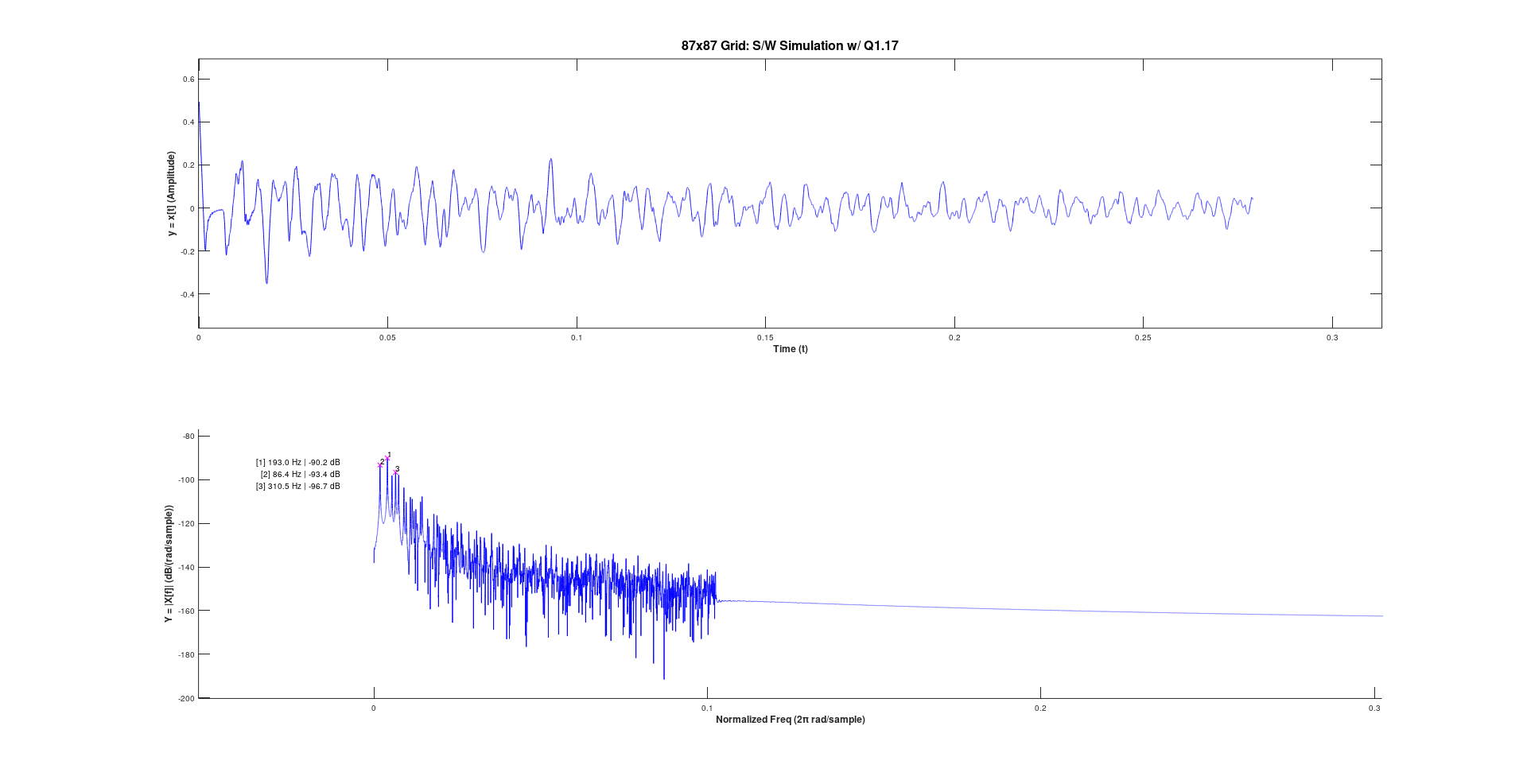
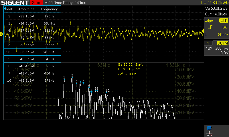
Frequency analysis of the software simulation detects 193.0 Hz, 86.4 Hz, and 310.5 Hz as the largest frequency components, and the oscilloscope measures 195 Hz, 85.4 Hz, and 311 Hz as the largest frequency components, which seem to agree with one another reasonably well.
Excitation and Sample Readback Memory
The HPS can add energy to the system (Analogous to setting the initial conditions of the simulation) by writing to the excitation memory. This is an additional two port BRAM bank which is written to by the HPS via an Avalon Bus Slave and read from by the compute engine. Every iteration the compute engine will read the value stored in the excitation grid for the given node into the excitation register to be used as part of the computation. Since this memory is dual port (1 port read 1 port write) it is the responsibility of the software application to modulate these values to avoid a feedback loop of the simulation. For example if you set the excitation grid to a value, then every iteration that energy will be accumulated into the result. This allows the HPS to implement any sort of complex excitation model to model some kind of mallet, but it needs to properly decay and clear the energy from this input. This is not a great solution as if the software application closes, then the simulation will become unstable and needs to be reset and restarted.
Additionally, the HPS can read back the simulation by reading from the so-called “sample memory”. This is another two port BRAM bank which is written to by the compute engine and read from by the HPS via an Avalon Bus Slave. The compute engine simply duplicates the result its writing back to the compute memory into this memory bank so the HPS can sample it.
There is an interrupt signal issued to the HPS indicating when the current iteration has completed, allowing the HPS to update the excitation grid, read from the sample memory, etc. In practice this never worked out quite correctly, as issuing memory stores to the BRAM via the Avalon Slave was extremely slow. I wasn’t sure if this was due to the lightweight bus, but it seemed like memory transactions stalled for a significant period of time when coming from the HPS. This means that writing to the excitation grid actually occurs over multiple iterations. Also, this interrupt method is not great when running linux because it introduces a real-time constraint, as we need to fill the excitation grid before the next sample begins, but we don’t have a way of guaranteeing our application’s thread will be executing. This would be more suited to a baremetal application.
VGA Scanout
The frame buffers are displayed on a VGA monitor. There are three main components to make this happen.
- An AXI master for reading from the SDRAM bank, which we are utilizing as video memory.
- A scan buffer to buffer each line scanned out to the VGA DAC
- Timing circuit to synchronize the VGA scanout with the monitor
Single Beat Pipelined AXI Master
Each frame has a resolution of 640x480 with a bit depth of 16 bits per pixel. In our case the AXI data interface is 32 bits wide, so this corresponds to 153600 32-bit words. The VGA pixel clock executes at 25 MHz, so we need an effective transfer latency from SDRAM of transferring one 32-bit word every 80 ns. i.e., if we were to buffer a single pixel every VGA clock cycle the transfer would need to complete in 80 ns. This includes the request latency on the AXI bus, the latency of the SDRAM controller and memory access, then the bus latency of transferring the result. The system clock operates at 120 MHz, so this corresponds to 9 sysclk cycles. This would absolutely not be feasible. I chose to implement a Pipelined Single Beat AXI Master. This is a very simple scheme which allows us to have multiple memory transactions in flight at once which allows us to absorb the latency. As long as the scanout buffer has space available we will issue new requests for subsequent addresses of the frame buffer. This allows the SDRAM reads to stay ahead of the scanout position.
The scanout buffer (discussed next) provides a Start of Frame (SOF) signal triggering the AXI Master to begin filling the scanout buffer with the next frame by reading from the frame buffer base address. The base address is a register programmed by the software application, allowing us to implement hardware double buffering.
Scanout Buffer
The scanout buffer is a clock domain crossing (CDC) FIFO written to by the AXI Master (system clock) and read from with the VGA clock. Reads from the CDC FIFO incur a latency of 2 cycles so the VGA control signals must be pipelined by 2 cycles. When the timing circuit is in the active portion of a scanline it will pop new pixels from the FIFO. One thing to note here is this still operates on 32-bit words, i.e., there are two pixels per word stored in the FIFO. I used a ‘phase’ clock which is simply a clock divider to divide the VGA clock in two, to only read one element every two VGA clock cycles, and output only the lower or upper 16-bit halfword to the VGA DAC.
VGA Timing Circuit
The VGA timing circuit simply counts VGA clock cycles and controls when the HSync, VSync, and Blank signals are high and low. I also expose a start of frame (SOF), end of frame (EOF), and an “Active Region” signal which indicates when the timing cycle is in the active region (i.e., should be scanning out pixels).
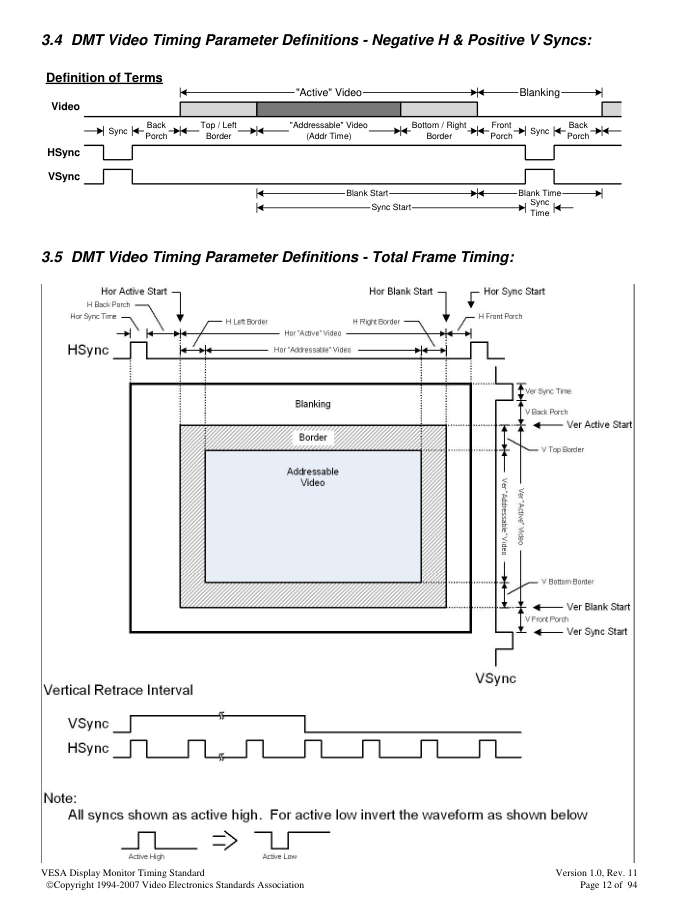
For a 640x480 display at 25 MHz I used the following timing parameters:
Horizontal Timings:
- Sync: 96 Cycles
- Back Porch: 48 Cycles
- Display Interval: 640 Cycles
- Front Porch: 16 Cycles
Vertical Timings:
- Sync Pulse: 2 Lines
- Back Porch: 33 Lines
- Display Interval: 480 Lines
- Front Porch: 10 Lines
Audio DAC and FIFO
In order for the simulation to be audible, we need a way to feed the result of the simulation to the audio DAC, which can then be connected to an amp/speaker. The simulation updates the position (amplitude) for every node in the grid each iteration, but we need to convert that into a 1D audio signal. I just did the simplest thing here and sampled the center node of the grid and output that directly to the DAC. A much more sophisticated approach would involve modeling sound pressure propagation and a microphone or some kind of diaphragm.
The DAC is interfaced via an I2C bus. Thankfully it is connected to both the FPGA fabric as well as the HPS, so we can just program the DAC from the software application rather than instantiating an I2C peripheral in the FPGA fabric. All that’s involved in making that happen is configuring a GPIO, which controls a multiplexer selecting whether that particlar I2C bus is controlled by the FPGA fabric or by the HPS. Once we can interface with the DAC from software, we can utilize the Linux I2C interface to configure the sample rate, bit depth, audio interface format (left justified in this case), etc.
I also implemented an audio FIFO which feeds a shift register to clock out the audio sample to the DAC. This utilizes a clock domain crossing (CDC) FIFO which crosses the system clock domain to the audio clock domain. The main idea here was to use the LR clock (which operates at the sampling frequency) to trigger when to pop a sample from the FIFO into a shift-register, and then shift it out on the serial data line. This is a bit tricky for a few reasons. First is that there are three different clock domains interacting here. One clock domain is the simulation clock domain. We already know we will need multiple cycles to compute the results for all the nodes (ergo, that clock speed must be faster than the audio sample rate). Another is the audio bit clock. The audio sample is ‘clocked out’ over a serial data line, which means we must clock out multiple bits during one audio sample period. And lastly, we have the audio ‘LR’ (left/right) clock which operates at the sampling frequency. So we have a clock domain crossing (CDC) from the simulation clock to the audio bit clock. This means we need an asynchronous FIFO, with the simulation clock domain feeding the write port, and the audio bit clock removing samples from the read port.
The other tricky part is that we need to utilize the LR clock to trigger when to clock out a new sample. If we take a look at the output format, we can see that the polarity of the LR clock is actually inverted with respect to the bit clock.
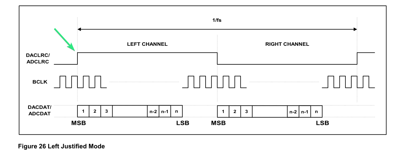
This means we can sample the LR clock with the bit clock. The data input port expects data on the first clock edge following the edge of the LR clock, which means we can’t wait to react to the edge, we must have data ready to go, so to speak. As we are waiting for the edge of the LR clock, we can continually load a sample into the shift register, then when we see the level of the LR clock change, we can trigger the shift register to shift out the data.
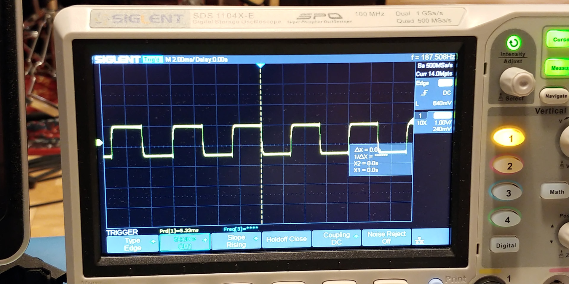
I successfully implemented and simulated this with little issue, and here’s a screen shot of a simple square wave output on the DAC (generated from the FPGA programmable logic)
Software
At a high level the software application performs the following tasks:
- Configuring audio DAC
- Transferring offscreen framebuffer to SDRAM for VGA scanout
- Polling mouse, implementing GUI with sliders for controlling simulation parameters
- Setting simulation parameters via IO registers in the FPGA fabric
- Triggering membrane excitation via writing to excitation memory
- Sample simulation results via sample memory and displaying to the screen
The embedded ARM HPS is a dual-core processor, so I chose to utilize one core for the GUI and another core for controlling the simulation/excitation memory, since we have some timing constraints on the excitation. There is a SPSC queue (single producer, single consumer) of events passing data from the GUI thread to the controller thread, which can contain ‘strikes’ initiated by the user, or updates to the simulation parameters.
The simulation control thread computes a linear displacement per time step to apply based on the amplitude of the strike made by the user as well as the amount of time to apply it over (convert time to samples then divide the amplitude by the number of samples). The strike event also contains information about the position and width/height of the ‘mallet. The thread generates a grid pattern based on these parameters and writes out the given per-time-step displacements to the excitation grid. It then sleeps for the duration the strike is applied (the divided value will will be accumulated per time step per node), then it will clear that area in the excitation grid back to zero.
Excitation Model
In order to make this an interactive piece, we need to be able to dynamically add energy into the system. A simple model is deployed here. When striking the surface of the drum, the stick (mallet) would transfer energy via a force applied to the membrane over a short period of time. i.e., we would expect a force to be applied over multiple iterations of the simulation, meaning that we don’t just have a single discrete jump in displacement of the drum over one time step. I took a look at an audio waveform from one of my snare drums and measured the duration of the ‘transient’ portion of a strike.
As shown here, it appears the transient occurs over a period of ~1 ms (50 samples), which is exactly what I expected (based on previous knowledge). Since a force is acting on the head to accelerate it, the force itself should not occur for this duration, because additional velocity would carry the membrane through to the maximum position. Based on this, I would guess that a force applied over 0.25 ms to 1.0 ms seems reasonable. I’m not trying to be super scientific here, just get something in the ballpark.
I wasted a day researching what had previously be done to model drum mallets in this context. The schemes were too complicated to feasibly implement in the hardware simulator at this point. I tried to devise a simpler scheme modelling a constant force (constant change in velocity) over a small time period, but it didn’t sound very good to me, and it was still not feasible to implement given that we only store two time steps of information. I decided to just model a simple constant velocity applied for a short duration resulting in a linear addition to the displacement over time.
I had previously come up with an incredibly simple scheme that would map nicely into the FPGA hardware. It looked something like this: We would dedicate an additional BRAM unit to each compute engine that stores energy to be dumped into the system. When computing the new displacement of a node for the next time step, it would add some portion of this energy from a pool (if there was any to add), and subtract it from the pool. But, I made a critical error here. We only have a single write port and a single read port for these memories. Since we want to write to this memory from the HPS (via a bus slave), we would then need to multiplex the write ports to the memories with the Compute Engine to allow it to subtract from the pool. This involves a bunch of additional complexity that I was not interested in.
Cached Software Rendering
Transferring the video frames to the “video memory” (external SDRAM) was taking a lot longer than expected. For reasons I still haven’t nailed down, the HPS seems unable to sustain high bandwidth memory transfers and just stalls out for (relatively) long periods of time. I’m not sure if this has something to do with backpressure applied by the SDRAM memory controller slave since it is not correctly pipelined. But, it still supports (amortized) 3-cycle writes, but I see something like 2 writes being issued by the HPS every ~24 cycles, which is not enough sustained bandwidth for writing the video frames.
I started exploring utilizing the embedded hard DMA Controller to transfer the video frames, as benchmarks from external sources indicated it is significantly faster than memory operations by the HPS itself. But, I quickly realized that this thing was way more complicated than I anticipated and likely to lead down a dark rabbit hole.
Instead, I decided to implement something akin to a ‘Cached Software Renderer’. This is typically utilized in software rendered GUI applications to avoid needlessly redrawing into a backbuffer when the actual pixel data is not being modified. I figured I could utilize a technique like this to only retransmit the portions of the framebuffer that had been modified. The jist of the technique is that the backbuffer is segmented into higher granularity chunks and a hash of drawing operations is kept per chunk. The idea is that the hash gives an ‘estimation’ of what pixel data exists in that chunk of the backbuffer, and you can check the hash of the previous frame to know if that chunk of the backbuffer has been modified. This hash is produced by taking the hash of all the parameters of a given drawing operation and mixing it with the hash that already exists for that chunk. If all the same operations are applied to a given chunk, then its hash won’t be changing from frame to frame. Then, when transmitting the newest frame to video memory, the hash of each chunk can be checked against the one for the previous frame to determine if a chunk needs to be retransmitted or not.
Hardware Double Buffering
The cached software rendering was still not quite sufficient in reducing the transmission time to reasonable levels for this application. Up to this point I was doing what I would call… ‘pseudo double buffering’, where there was only one framebuffer in video memory that was scanned out to the monitor. On the V-Sync signal I would transfer a new frame to the video front buffer. But, this only works if the new frame can be transmitted infront of where the scan out is ocurring on the monitor. Due to the still slow transfer rate, the scan out was occurring faster than the transmit, causing screen tearing artifacts as the scan out position exceeded the write position.
Thus, I finally implemented real hardware double buffering. This was pretty simple by exposing a register with a base address of a framebuffer to the HPS, and then using that as a base address for the video scan out circuit. One gotcha here is that since we are no longer transmitting the entire video frame every time, we have to update both of the frame buffers in video memory. The order of operations look something like this:
- Perform updates for current frame of application, issuing drawing operations to the (CPU allocated) back buffer and generating chunk hashes
- Transmit current frame diff (based on hashes) to the video memory back buffer
- Wait for the V-Sync signal
- Update the base address of the frame buffer in the video controller to make the back buffer the front buffer
- Transmit current frame diff (based on hashes) to the new video memory back buffer
- Swap the front and back buffers (from the software’s perspective)
Funnily enough this somewhat undoes the work done for the cached rendering, as if we were transmitting the entire frame everytime, we wouldn’t need to effectively copy the data to both frame buffers. But, I think it’s still a savings over all as most of the screen is not being interacted with.
SDRAM Memory Banks
I also have an example to share about acquiring deep knowledge of topics and leveraging that for better decision making.
When I was creating the memory controller from scratch, I was able to reify my understanding of how DRAM memory functions at a fundamental level. DRAM is actually quite slow due to a fundamental opposition of goals of memory density and speed. (Skipping some details here) DRAM arrays are organized into rows and columns, and require a specialized circuit called a ‘sense amplifier’ to read and write the memory. The sense amplifier ‘amplifies’ the data seen on a given row of the array (this is called opening a row). Only one row can be open at a time in the array, and if you want to open a new row, you must first spend the time to ‘close’ the previous row by recharging the memory cells for that row, then spend the time opening the new row. These are multiple wasted clock cycles doing nothing. The consequence of this is that you can not just read and write any cell willy nilly. From creating the memory controller I also learned that the DRAM IC contains multiple banks of memory, each with their own set of sense amplifiers. This means you can effectively have four different rows open from different banks simultaneously.
Utilizing this knowledge I knew it was better to place different framebuffers NOT sequentially in the memory (which might be the intuitive thing to do), and instead place them in separate memory banks. This way when there is contention from multiple masters for reading/writing the memory, they are not constantly stepping on each others toes wasting time opening and closing different rows that are far away, but still in the same bank of memory. i.e., when the video manager will be scanning out the front buffer to the monitor, and the data for the next frame is being written to the back buffer, they will only be contending for the memory interface, but they won’t be contending for the memory banks internal to the DRAM IC, saving a significant amount of time!